 janikandClaude Fable 5
26b1cfaa45
janikandClaude Fable 5
26b1cfaa45
Multiple Thevenin supplies and prescribed-current loads on one net,
solved in absolute volts with the Tellegen power balance verified per
run; a source-sink pair table (effective copper resistance per
supply x load pair plus an exactly-summing proportional-sharing loss
attribution), in summary.txt and as its own figure. Bonded terminals
short a package's contacts into one lug so the per-pin split becomes
a solve outcome. Geometry dumps carry the terminal set (schema v8).

The dialog gained a Classic/PDN mode selector and a full PDN editor:
per-role supply/load tables built from the marker rectangles (or a
config's terminal set, which never pins mode or net), with Component
hints, per-terminal Layer scopes, Active checkboxes, comments, a
per-net row filter, resizable tables and a scrolling, screen-sized
dialog. Numbers accept SI suffixes (50m, 4.7k) everywhere.

fill_res_config.json fully specifies a run (classic or PDN) with
validation, comments, named side-by-side configs (the one called
default auto-loads), Load/Save buttons with an editable file name,
and saves that never drop anything drawn on the board.

347 tests, green on Python 3.13 and on the 3.9 macOS wheel stack.

Co-Authored-By: Claude Fable 5 <noreply@anthropic.com>
41 KiB
Fill Resistance — KiCad 10 plugin
Computes the DC resistance of copper zone fills and traces between two contacts, single- or multi-layer: the chosen net's fills (teardrops included) and tracks on the selected copper layers are solved as coupled finite-difference sheets linked by the net's via and through-hole-pad barrels (18 µm plating, configurable). Shows per-layer rasterized maps, potential, current density, and power density, and reports per-via currents (via ampacity!) and total dissipation at a selectable test current.
PDN mode replaces the single driven pair with a whole power rail: any number of supplies (Thévenin sources with configurable output resistance and open-circuit voltage) and loads with prescribed current draws on one net — set up from marker rectangles in an editable dialog or a JSON config — reporting the IR-drop map, per-supply current sharing and per-load contact voltages in absolute volts.
PNGs + a text summary are saved per run. An optional skin-effect correction (exact 1D foil/barrel solution at a user-set frequency) estimates the resistive skin rise only — it is not an AC impedance simulation (no proximity effect, no inductance; see Model & limits).
 Real output on a synthetic two-layer net: current from a soldered
THT-pad contact (V+, injected at the drill-wall ring) squeezes past a
notch in the F.Cu pour, transfers through the stitching-via field into
the B.Cu pour and leaves at the V− lug. Per-via currents and the
hottest via are reported.
Real output on a synthetic two-layer net: current from a soldered
THT-pad contact (V+, injected at the drill-wall ring) squeezes past a
notch in the F.Cu pour, transfers through the stitching-via field into
the B.Cu pour and leaves at the V− lug. Per-via currents and the
hottest via are reported.
 The matching potential map with equipotential contour lines: they
bunch where the field is strongest — nearly the whole 8.7 mV drop
happens around the notch on F.Cu.
The matching potential map with equipotential contour lines: they
bunch where the field is strongest — nearly the whole 8.7 mV drop
happens around the notch on F.Cu.
Uses the KiCad IPC API (kicad-python / kipy), not the deprecated
SWIG API. Requires KiCad 10.0.1+.
Platform support

| Platform | Status | Verified by |
|---|---|---|
| Windows | ✅ | development platform, full suite before every release |
| macOS | ✅ | field-tested in KiCad 10 |
| NixOS | ✅ | field-tested in KiCad 10 (setup) |
| Debian 12 | ✅ | CI test suite in container |
| Ubuntu 24.04 | ✅ | CI test suite in container |
| Fedora (latest) | ✅ | CI test suite in container |
| Arch (latest) | ✅ | CI test suite in container |
CI (.gitea/workflows/ci.yml) runs the full pytest suite — solver,
rasterizer, and the platform-fallback regressions — headless against
the real pip wheels of each Linux row, including the
PySide6.QtWidgets import probe that decides the matplotlib backend.
What CI cannot do is launch KiCad itself, so "runs inside KiCad"
remains field-tested (Windows continuously, macOS and NixOS per
release).
Setup (one-time)
The plugin is developed and tested on Windows; macOS works
(field-tested on KiCad 10 after a round of mac-specific fixes), and
Linux works (field-tested on NixOS — the hardest Linux to run pip
wheels on; mainstream FHS distributions should be no harder, reports
welcome). KiCad builds the plugin a private Python venv from
requirements.txt on every platform, from pre-built wheels only, no
compiler needed. Steps 1–4 are the same everywhere; OS specifics are
spelled out per step and in Platform notes below.
- Enable the API server: KiCad → Preferences → Plugins → check Enable KiCad API.
- Check the interpreter path on the same page (after a 9→10
upgrade it can still point at KiCad 9):
- Windows: KiCad's own Python,
C:\Program Files\KiCad\10.0\bin\pythonw.exe; - macOS: the Python bundled inside the app,
/Applications/KiCad/KiCad.app/Contents/Frameworks/Python.framework/Versions/Current/bin/python3; - Linux: the first
python3onPATH— needs Python ≥ 3.9 with thevenvmodule (Debian/Ubuntu:sudo apt install python3-venv).
- Windows: KiCad's own Python,
- Deploy (dev checkout; end users install the PCM zip instead, see
Packaging / publishing). Windows:
Linux / macOS (also works on Windows with developer mode):
powershell -ExecutionPolicy Bypass -File deploy.ps1 # junction (dev) powershell -ExecutionPolicy Bypass -File deploy.ps1 -Mode CopyPlugin directory:python3 tools/deploy.py # symlink (dev) python3 tools/deploy.py --copyDocuments/KiCad/10.0/pluginson Windows and macOS,~/.local/share/kicad/10.0/pluginson Linux. - Restart KiCad; first load builds the plugin venv (numpy, scipy,
matplotlib, PySide6 — takes minutes; the Ω button appears when done).
If stuck: in the PCB editor, Preferences → PCB Editor → Action
Plugins, right-click the plugin's row → Recreate Plugin
Environment (context menu only — there is no button). Manual
equivalent: delete the plugin's venv and restart KiCad —
- Windows:
%LOCALAPPDATA%\kicad\10.0\python-environments\th.co.b4l.fill-resistance - macOS:
~/Library/Caches/kicad/10.0/python-environments/th.co.b4l.fill-resistance - Linux:
~/.cache/kicad/10.0/python-environments/th.co.b4l.fill-resistance
- Windows:
Platform notes
- Windows is the development and test platform — everything in this README was exercised here. KiCad's bundled Python is 3.13, so the venv gets the current dependency stack.
- macOS — works (field-tested on KiCad 10). Requires macOS 12+ (KiCad's own minimum; Intel and Apple Silicon — the dmg is universal). KiCad's bundled Python is 3.9, so pip resolves an older stack (numpy 2.0, scipy 1.13, matplotlib 3.9, PySide6 6.9/6.10); the plugin code is kept 3.9-compatible (guarded by a test) and the suite is also run against that older stack. Plot and dialog windows may open behind the KiCad window (they are raised best-effort) — check the Dock if nothing seems to appear after a solve.
- Linux — works (field-tested on NixOS, KiCad 10; mainstream
distributions are audited but not yet field-tested). The venv uses
the system Python (3.9+), so the stack matches your distribution.
On ARM64 (aarch64) there are no pyamg wheels —
requirements.txtskips pyamg there and the solver falls back to Jacobi-CG: same results, noticeably slower on large grids. NixOS: works (field-tested on NixOS 26.05, Plasma 6). pip's Linux wheels link against standard FHS library paths, which NixOS does not provide — PySide6 fails withlibgthread-2.0.so.0: cannot open shared object file. The plugin cannot fix this from inside its venv (KiCad installs wheels only); run KiCad inside an FHS environment built withbuildFHSEnv, and — on KDE Plasma — unsetQT_PLUGIN_PATH, which otherwise poisons the wheel's bundled Qt with the system's Qt plugins. The tested wrapper (exact package list incl. the non-obviouszstd.outand xcb-util family), asteam-runquick test, and a debugging guide are in docs/NIXOS.md.
Usage
- Mark the current-injection terminals. Each terminal may have
multiple parts (all merged into one externally bonded contact):
- V+ rectangles on
User.1, V− rectangles onUser.2(marker layers, configurable viaELECTRODE_POS_LAYER/ELECTRODE_NEG_LAYER), any number per side, axis-aligned; - pads and vias (SMD pad: real copper shape on its own layer;
through-hole pads and vias become barrel contacts: the current
enters at the drill wall on every spanned layer, see below).
Selected pads/vias fill the side that has no rectangles, so
mixing both kinds is the everyday workflow: e.g. select one
rectangle on
User.1(V+) plus any number of pads / THT holes (Ctrl-click) — the pads together form the V− terminal (a connector's pin group, a via cluster, …). All selected pads/vias go to that one side; if both marker layers already provide rectangles, selecting pads on top is an error; - legacy: exactly 2 selected contacts with no marker rectangles still works; empty selection scans the whole board's marker layers.
- V+ rectangles on
- Select the contacts, click the Fill Resistance Ω button.
- In the dialog, pick the net (defaults to the selected pad's net), check the layers to include, set each contact's layer scope ("All selected layers" = bolted-lug/through contact), the test current, and optionally a grid cell size. Multiple layers are coupled through the net's via/pad barrels automatically. The Mode selector at the top switches to PDN mode — per-terminal currents instead of one driven pair — when rectangles exist on both marker layers or a config file provides the terminal set.
- Wait for the solve. Depending on board size, included layers, cell
size and your hardware it can take considerable time — large
multi-layer pours at fine cell sizes may run for minutes (on our
test setup a typical real-board run finishes in ≈ 8 s). Then read
R / voltage drop / total power in the figure titles and status
bar. Outputs land in
<board dir>/fill_res_results/<timestamp>/(if the board directory is not writable — e.g. a demo project opened straight from the mounted installer image — a temp directory is used instead and its path printed to the Messages panel): per-layer1_raster_map/2_potential/3_current_density/4_power_densityPNGs (PDN runs add5_source_sink_pairs, the pair table as a figure),summary.txt(incl. the busiest vias with per-via current and dissipation, and the current through each injection area — computed flux with the equipotential model, prescribed area share with the uniform model),geometry_dump.json. - Experimental — overlays inside KiCad (dialog checkbox, default
off; KiCad ≥ 10.0.1): after the solve, the per-layer |J| heatmaps
are pushed into the open board as unlocked reference images on
User.9…User.12(OVERLAY_LAYERS; enable them in Board Setup), copper layers mapped in stackup order, top first. Toggle them in the Appearance panel like any layer; opaque over copper, transparent elsewhere, cold end lifted so it stays visible on the dark canvas. Reference images never plot to gerbers. Every push replaces all reference images on those layers, so don't store unrelated images there. Also available headless:python tools/kicad_heatmap_overlay.py --net X --amps 10. - Experimental — low-current copper marking (dialog checkbox,
default off): after the solve, the copper whose |J| is below a
threshold is outlined as filled graphic polygons on user
layers. The threshold is dialog-settable in one of two units
(selector next to the field): relative — % of the mean |J| over
all solved copper (default, 10 %) — or absolute in A/mm²;
since |J| scales with the test current, the absolute variant is
meant to be used with the real operating current entered as test
current. Polygons land on
User.5…User.8(TRIM_LAYERSinfill_resistance/config.py; enable them in Board Setup), copper layers mapped in stackup order, top first. Marked specks underTRIM_MIN_AREA_MM2(0.5 mm²) are dropped. Each region is one selectable polygon — use KiCad's Edit → Convert to turn one into a rule area or zone cutout by hand. Per-layer areas are printed to the Messages panel and the polygons also land inlow_current_copper.jsonnext to the PNGs. Every push replaces all graphic polygons on those layers (one undo step). This is a suggestion, not a safe cut list: copper carries little current because the rest carries it — removing copper redistributes the current and raises |J| everywhere else, so re-run after any change. The pour may also serve thermal spreading, EMI return paths, or plane capacitance, which this DC analysis does not see.
Configuration file
The plugin optionally reads a JSON config next to the board file. It can fully specify a run — the shared run parameters, the classic setup (optionally including the terminals themselves, by board reference), or the PDN terminal set.
Named configs: several configs can live side by side as
fill_res_config.<name>.json; the config named default loads
automatically. Search order on launch:
<board stem>.fill_res_config.json (board-specific — several boards
can share a directory), then fill_res_config.default.json, then
plain fill_res_config.json (the legacy spelling of "default"). Any
other config is pulled in per run with the dialog's Load config…
button (a file picker starting in the board directory): the dialog
re-opens with everything — mode, net, terminals, values — taken from
the picked file. Save config… asks for the target file name each
time (pre-filled with the loaded config), so writing back and saving
a variant under a new fill_res_config.<name>.json are both one
click — a name outside the auto-load set prints a reminder that it
needs Load config….
Precedence: config.py constants < config file < dialog edits.
The file pre-fills the dialog; what the dialog shows is what runs. A
missing file changes nothing; a present-but-invalid file stops the run
with a readable error (never a silent fallback). The Save config…
button in the dialog writes the current dialog values back to the file
(creating it if needed) — in classic mode the run parameters and
terminals-by-reference, in PDN mode the whole terminal set — so "run
once, tweak, save" is the whole authoring workflow.
Format notes: plain JSON, but full-line comments starting with
// are allowed, and keys starting with _ are ignored everywhere
("_comment": "..."). Unknown keys print a warning (typo guard) but
don't stop the run. Units are plain SI floats (A, Ω, V, Hz), _mm
keys are board millimetres, _um metal micrometres. Any number may
also be written as a string with an SI suffix — "50m" = 0.05,
"4.7k" = 4700, case separating m (milli) from M (mega) — and the
dialog's number fields accept the same suffixes typed directly
(50m for a 50 mΩ R_out). freq_hz keeps the frequency grammar
("142k", "1.5M"; a lone m means MHz there).
A classic example (docs/fill_res_config.example.json):
{
    "version": 1,
    "mode": "classic",
    "run": {
        "net": "VOUT+",
        "layers": ["F.Cu", "In1.Cu", "B.Cu"],
        "freq_hz": "142k",
        "adaptive": true,
        "trim": {"enabled": false, "mode": "pct", "value": 10.0}
    },
    "classic": {
        "current_a": 40.0,
        "pos": ["J1.1"],
        "neg": ["J2.1", "J2.2"]
    },
    "physics": {"via_plating_um": 25.0}
}
Every run key is optional and mirrors a dialog field
(include_tracks, vias_capped, cap_max_drill_mm, adaptive,
cell_um, freq_hz, contact_model, include_buildup,
extra_cu_um, push_overlays, v_nominal, trim). classic.pos /
classic.neg define the terminals by reference — when present,
the board selection / marker-rectangle scan is skipped entirely and
run.net is required. The reference grammar (shared with PDN
terminals):
| form | meaning |
|---|---|
"U7" |
every pad of footprint U7 that is on the run net |
"U7.3" |
pad "3" of U7 (split at the first dot — pad numbers are strings and may contain dots) |
"rect:NAME" |
rectangle on User.3 named by a text item placed inside it |
{"rect_mm": [x0, y0, x1, y1], "contact": "F.Cu"} |
explicit rectangle, board mm |
{"via_mm": [x, y]} |
the net's via nearest to (x, y), within 1 mm |
physics overrides the constants you'd otherwise hand-edit in
config.py (rho_cu_ohm_m, copper_thickness_um, via_plating_um);
markers renames the marker layers (pos_layer, neg_layer,
pdn_layer). The full schema is documented in
fill_resistance/configfile.py.
PDN mode
For power-distribution studies the plugin can replace the single driven
terminal pair with multiple supplies and loads on one net: each
supply is a Thévenin source (open-circuit voltage v_oc behind
r_out_ohm), each load draws a prescribed current i_draw_a. The
solve then runs in absolute volts: supply currents fall out of the
Thevenin split, and you get the IR-drop map, per-supply delivered
current and per-load voltage (mean and worst-case) in summary.txt
and the figures.
The summary also carries a source-sink pair table: for every
supply × load pair, the effective copper resistance between the
two contacts (an operating-point-independent board property — source
R_out excluded, contact patterns as in the solve, one extra linear
solve per terminal, deferred-corrected on the adaptive grid too) and
the copper loss attributed to the pair by proportional sharing
(f_ij = I_i·I_j / I_loads, per copper island). The attribution is a
convention — the pairwise flow split is not unique physics — but it
sums exactly to the total copper dissipation, never crosses a
copper gap, and pairs without a common copper path report "no path".
The same table is also rendered as its own figure
(5_source_sink_pairs.png) next to the field maps.
There are two ways to set a PDN run up: the dialog editor (marker rectangles, no JSON needed) or the config file.
The dialog editor
Draw supply rectangles on User.1 and load rectangles on
User.2 — the same marker layers as classic mode, but in PDN mode
each rectangle is its own terminal (classic merges each layer into
one V+/V−). Optionally place a text item inside a rectangle to
name it; unnamed rectangles get automatic names (S1, S2… / L1, L2…).
Launch the plugin and switch the Mode selector at the top of the
dialog to PDN: two tables — Supplies and Loads, each titled
with the marker layer its rectangles come from — list one row per
rectangle with its role taken from the layer. Only rectangles whose
copper belongs to the selected net are shown: switching the net
swaps the visible set, a count of hidden rows appears under the
tables, and hidden rows take no part in the run (not validated, not
solved). They are still saved, though: Save config… writes every
rectangle to the file — off-net ones as "active": false, values and
comments included — so nothing set up in the dialog is ever lost by a
save. Config-backed runs apply the same per-net filter, so such
archived terminals are skipped per run, never an error. A read-only
Component column identifies each row by the footprint whose pad
intersects the contact rectangle (e.g. U5); when no pad touches it,
the nearest component is shown as near U5. You type each load's
current draw and each supply's output resistance (plus an optional
per-supply V_oc; empty = the V nominal field below the tables).
Every row also has a Layer combo picking the copper the terminal
contacts — All selected layers (a rectangle's natural scope: a
bolted-lug/through contact) or one specific layer, exactly like the
classic contact scopes. The tables size themselves to their
rows and are height-resizable (drag the divider between them, or
enlarge the dialog); in PDN mode the dialog opens at ~60% of the
screen height so the tables start with room, and when the form
outgrows the screen the dialog scrolls, with the buttons always in
view. An Active checkbox per
row disregards a
terminal for what-if runs without deleting anything: an unchecked row
takes no part in the solve, may leave its value cells blank, and is
still saved (as "active": false) so it can be re-enabled later — the
totals line counts disabled rows. A free-text Comment column
annotates each terminal and is saved along with it. Rectangles that share one name
become a single bonded terminal — one table row, one total
current, and the per-rectangle split is a solve outcome (a multi-pin
package whose pins are joined by internal metal: the total draw is
known, which pin carries how much is exactly what the solve
determines). OK solves;
Save config… writes the whole setup to a config file whose name
you pick per save (pre-filled with the loaded config, else
fill_res_config.json) so the values survive between runs — named rectangles are saved as live rect:NAME
references (they follow the rectangle wherever it moves), unnamed ones
are frozen as rect_mm coordinates, so label your rectangles if
the layout is still moving. A saved config provides the terminal
set: the next launch opens in PDN mode (the saved mode is only the
starting mode — nothing is pinned, the Mode selector and the net
stay switchable) with the geometry read-only, everything else
editable. Newly drawn rectangles still show up: any marker
rectangle the config doesn't reference yet appears as a fresh
terminal row (a note under the tables counts them), and Save config…
appends it to the file; a rectangle named after an existing
rect:NAME terminal instead joins that terminal as another contact
part (add "bonded": true in the file if those parts are internally
joined). Delete the config's terminals section (or the file) to
return to the pure live scan. In a directory where
several boards share fill_res_config.json, save to the
board-specific <stem>.fill_res_config.json instead. Rectangle names
must be unique across User.1/User.2/User.3. The board selection
is ignored in PDN mode (terminals are the rectangles; pads/footprints
as terminals need the config file).
The config file
The config file can express everything the editor can, plus terminals made of pads and footprints (reference grammar above). A PDN example (docs/fill_res_config.pdn.example.json):
{
    "version": 1,
    "mode": "pdn",
    "run": {"net": "VCC_3V3", "v_nominal": 3.30, "adaptive": true},
    "terminals": [
        {"name": "buck", "role": "supply",
         "parts": ["U1.SW2", "U1.SW3"], "r_out_ohm": 0.004},
        {"name": "ldo", "role": "supply",
         "parts": ["U2.OUT"], "r_out_ohm": 0.050, "v_oc": 3.28},
        {"name": "mcu", "role": "load", "parts": ["U7"],
         "i_draw_a": 1.8, "bonded": true},
        {"name": "cam", "role": "load", "parts": ["rect:CAM_ZONE"],
         "i_draw_a": 0.35, "contact": "F.Cu"}
    ]
}
run.netis required; every terminal needs a uniquename, arole(supply/load) and non-emptyparts(reference grammar above). Active loads needi_draw_a(≥ 0; 0 = voltage probe), active supplies needr_out_ohm(0 = ideal source) and optionallyv_oc(default:run.v_nominal, default 3.3 V). With one supply — or all supplies at the samev_oc— that voltage is only the absolute reference (drops and currents don't depend on it); with several supplies at differentv_oc, the differences drive the current sharing between them, so per-supply setpoints matter."active": falsekeeps a terminal in the file (and in the dialog, unchecked) without it taking part in the run — its value may then be omitted;"comment"is a free-text note shown in the dialog's Comment column."bonded": trueshorts all of a terminal's contact cells into one lug (a package with internal metal): the total value stays prescribed, but the per-part/per-cell split becomes a solve outcome and the contact face is equipotential. Without it (the default), a multi-part load splits its draw by area share and a multi-part supply attaches itsr_out_ohmper cell. Use bonded for "all pads of U7 draw 1.8 A total, per-pin unknown"; use the default for genuinely distributed draws (a heater area on a plane). A bonded load may even span disconnected copper sheets — the bond is the connection.- Area terminals (a plane region rather than pads): draw a
rectangle on
User.3(markers.pdn_layer) and place a text item inside it — the text names the rectangle forrect:NAME(rectangles have no name of their own in the IPC API). One layer serves supplies and loads alike; the role comes from the config. - On launch the plugin resolves every reference against the board and
shows the terminal tables in the dialog with the geometry read-only
(a config file is authoritative for which terminals exist) but
everything else editable — the I / R_out / V_oc columns, the
Layer scope, the Active checkbox, the Comment, the net, and the
Mode selector itself (the file's
modeis only where the dialog starts; switching to classic and saving keeps the terminals section intact). Tweak a value, OK runs with it, Save config… writes it back. The Layer combo edits the terminal-levelcontactkey (part-level contacts insidepartskeep winning, per the schema); structural edits (adding terminals, changing parts) happen in the file. - Contact models are fixed in PDN mode: supplies attach through their output resistance (per-cell equal conductances), loads inject uniformly (the classic "uniform" model). The contact-model setting is ignored with a note.
- Current must be able to flow: every load must sit on copper
connected to at least one supply (through vias counts), and a load
spanning disconnected sheets is an error. Two supplies with unequal
v_ocon the same copper exchange a circulating current — that is physics, not a bug. power balanceinsummary.txtis the Tellegen check: source power = copper loss +r_outloss + load power. Atfreq_hz > 0all draws are assumed in phase (worst case), same skin-only caveats as classic AC.- The
geometry_dump.jsonof a PDN run embeds the full terminal set (schema v8), sostandalone.pyre-solves it offline with no extra flags; older dumps load unchanged.
Model & limits
-
Sheet model per layer: R□ = ρ/t, ρ = 1.68e-8 Ωm (20 °C), t from the board's physical stackup. Layer z-positions from the stackup drive the barrel lengths.
-
Via/pad barrels: thin-wall annulus, R = ρ·L/(π·d·t_plating),
VIA_PLATING_UM = 18infill_resistance/config.py(orphysics.via_plating_umin the config file). Vias are always plated. Each via also contributes its ring/pad copper (a full-thickness disc of the pad diameter on every spanned layer) and its drill mouth, area-weighted per cell: with the "vias filled + capped" checkbox (default on,VIAS_CAPPED) the mouth carries a thin copper cap (CAP_PLATING_UM = 15, fab spec) on the outer layers and is an open hole on inner layers; unchecked, mouths are open holes everywhere. The fab caps only small vias: drills above the dialog's "capped up to drill" threshold (defaultCAP_MAX_DRILL_MM = 0.5) keep open mouths even with capping selected. Layer-to-layer the cap never matters at DC (it is in parallel with the annular-ring contact, not in series), so the checkbox only affects in-plane conduction across outer-layer mouths. Sub-cell mouths scale their cells' sheet conductance by the true covered fraction (4×4 supersampling), so coarse grids see the correct small perturbation instead of a whole-cell hole. Barrels are gathered in single-layer runs too (drill mouths perforate a lone plane). THT pads are fully modeled: their exact copper shapes (incl. oblong pads, fetched from KiCad; the outer shape stands in for inner rings) are stamped onto every included layer, and every populated pad carries its full soldered joint on its SOLDER side (opposite the component; the component-side pad face stays bare). The hole holds the component lead (a cylinder of drill −THT_LEAD_CLEARANCE_MM, resistivityTHT_LEAD_RHO_OHM_M, copper by default; raise it for brass/steel leads) plus solder in the remaining annulus, both in parallel with the plating. The filled hole also conducts in-plane on every spanned layer (component side and inner layers included): the mouth keeps its copper and additionally carries the plug — lead disc plus solder bore — as conduction-equivalent copper of the full hole depth (the pin continues beyond both mouths, so each layer sees the whole plug cross-section). The joint is side-symmetric except for the solder: coat and cone on the solder side only. On the raster map these mouths render in a darker tin color. The pad face gets the average-thickness solder coat (exact pad shape) and the protruding-lead cone (see barrel contacts below; on oblong pads the cone tapers to the pad's short dimension). Slotted (oval) holes keep their true stadium shape: the barrel wall, drill mouth, contact ring and lead cone all follow the slot (rotated with the pad), and the barrel conducts over the slot's real perimeter/bore area — not a circle of the slot's long dimension. Whether a hole is a via or a THT pad, the owning footprint's side, and its Do not populate flag are all read from KiCad. DNP pads get an open hole and a plating-only barrel, no joint. At f > 0 the thickness scaling is applied multiplicatively to the skin-corrected sheet conductance (approximation). Per layer a barrel attaches to the fill cell under it, or to the nearest copper cell within the pad footprint plus one grid cell — fills joined by thermal-relief spokes still connect; wider antipads do not, and the barrel bridges the layers above/below with the full barrel length. Barrels that reach fill on fewer than two layers carry no current and are reported.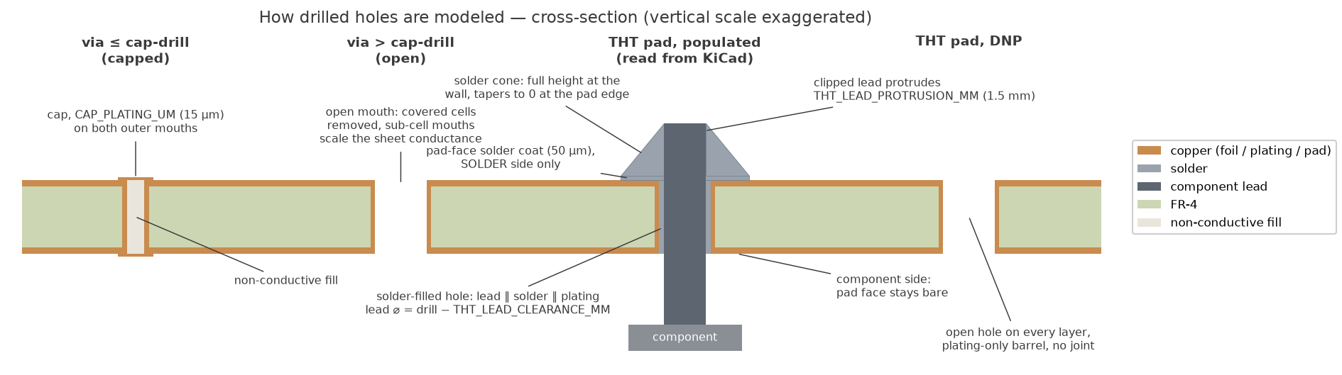 The four hole types: capped small via, open large via, populated THT
pad with its full solder joint (lead ∥ solder ∥ plating in the hole,
one-sided pad coat, protruding-lead solder cone), and a DNP THT pad.
The four hole types: capped small via, open large via, populated THT
pad with its full solder joint (lead ∥ solder ∥ plating in the hole,
one-sided pad coat, protruding-lead solder cone), and a DNP THT pad. -
The net's traces (straight and arc tracks, exact outline polygons incl. rounded ends) conduct together with the fills — dialog checkbox, on by default (
INCLUDE_TRACKS). Traces narrower thanTRACK_1D_FACTOR(3) grid cells are modeled as exact 1D resistor chains along their centerline — true arc length per link, so their series resistance carries no discretization error and no cell-size tuning is needed for thin traces. 1D-modeled traces show potential, power density, and |J| (the true in-trace density from the link currents, |ΔV|/(ρ·Δl)). Pad copper is part of the conductor: THT pad shapes are stamped on every included layer (see above), SMD pad shapes on their own layer (INCLUDE_SMD_PADS) — pads are the junctions where traces and thermal-relief spokes actually meet, so without them a multi-track junction necks down to the accidental overlap of the track ends. Dead-end pads (component terminals) are dropped with the other copper not connected to both contacts. -
Solder buildup on mask openings (dialog checkbox, off by default;
INCLUDE_MASK_BUILDUP): zones drawn onF.Mask/B.Maskare treated as mask openings that collectSOLDER_THICKNESS_UM(50 µm) of solder on the exposed pour, plus an optional user-defined added copper thickness (dialog field, e.g. a soldered busbar/wire). The sheet conductance there becomes t_Cu/ρ_Cu + t_solder/ρ_solder + t_extra/ρ_Cu (SAC305 ρ = 1.32e-7 Ωm: 50 µm solder ≈ 6.4 µm copper); interface faces use harmonic-mean conductances. Buildup areas render tin-gray on the raster map; |J| in them is referenced to the conductance-equivalent copper thickness. -
Barrel contacts: a selected via or through-hole pad injects at the drill-wall ring on every layer the barrel spans — the current physically enters through the lead/wire soldered into the hole, so the spreading resistance across the pad and surrounding pour is part of the result (both contact models; verified against R = ρ/(π·t)·acosh(d/2a) for two circular contacts on a sheet). Slotted holes inject along the stadium-shaped slot wall. A soldered THT joint additionally assumes the hole is filled with solder (core in parallel with the plating) and the pad face on the solder side carries an average-thickness solder coat (
SOLDER_THICKNESS_UM, 50 µm) over the modeled copper under the pad shape — the solder side is the side opposite the component (taken from the owning footprint; assumedB.Cuif it cannot be found), and the component-side pad face stays bare. There the clipped lead protrudesTHT_LEAD_PROTRUSION_MM(1.5 mm, 0 = off) and a solder cone wraps it: full protrusion height at the drill wall, tapering linearly to zero at the pad edge, applied as extra conduction-equivalent copper per cell. The tall solder column at the wall pulls the joint vicinity to lead potential — equivalent to extending the barrel wall vertically — while the taper carries the radial spreading. To model a probe pressed onto the pad face instead, draw a marker rectangle over the pad. -
Contact models (dialog /
CONTACT_MODEL): default uniform injection — a conductor pressed on top feeds the current orthogonally with uniform surface density, so |J| ramps across the contact area (R = ΔV̄/I from area-averaged terminal potentials); or equipotential — ideal bonded lug (Dirichlet). The two bracket a real contact: R_equipotential ≤ R_real ≤ R_uniform. If the selected fills form several disconnected copper groups that each touch both terminals (e.g. planes joined only through the bolted lugs), only the equipotential model is well-defined; the uniform model stops with an error instead of prescribing an arbitrary split.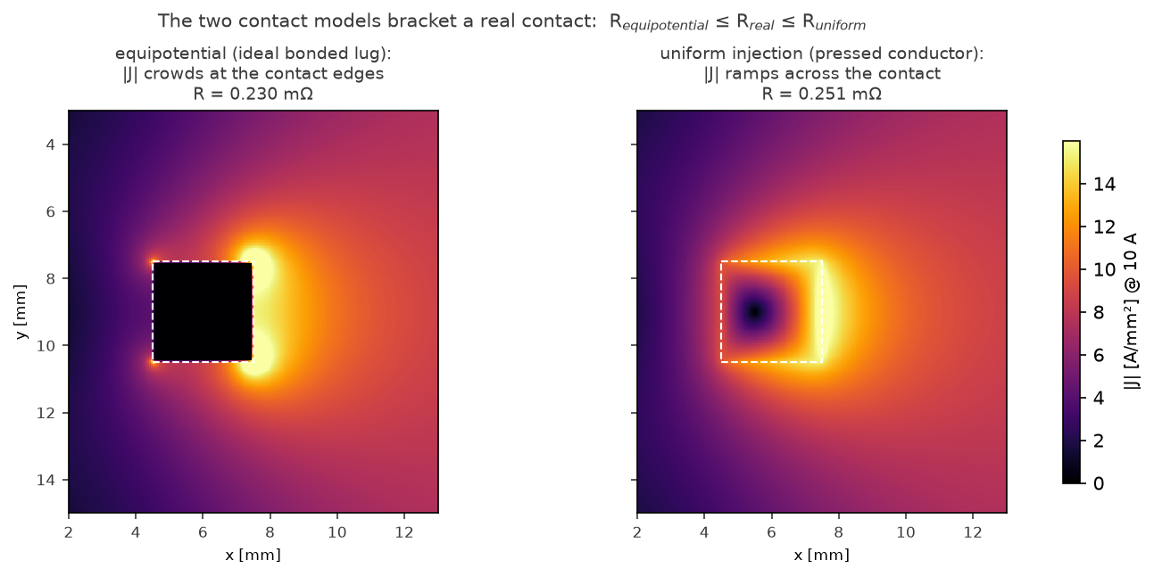 |J| around the same 3×3 mm contact under both models: the ideal
bonded lug crowds the current at the contact edges (no in-sheet
current inside an equipotential region), the pressed conductor ramps
it across the contact area.
|J| around the same 3×3 mm contact under both models: the ideal
bonded lug crowds the current at the contact edges (no in-sheet
current inside an equipotential region), the pressed conductor ramps
it across the contact area. -
Fields are reported at the dialog's test current; power scales with I².
-
Skin effect (f > 0): per-layer effective sheet resistance from the exact 1D foil-diffusion solution
Zs = τρ·coth(τt),τ = (1+j)/δ(SKIN_SIDES = 1in config: plane facing a return plane;2= isolated foil), and the analogous correction for the 18 µm barrel wall. Enter one frequency per run (e.g. a switching harmonic, with its RMS amplitude as the test current); suffixesk/Mare accepted. Caveat: this is not an AC impedance simulation — skin resistance is only a small part of real AC behavior. Only through-thickness crowding is modeled: lateral (proximity-effect) redistribution needs a magneto-quasistatic solver and is not captured — since the resistance-driven distribution is the minimum-dissipation one, the f > 0 resistance is a rigorous lower bound — and inductance, usually the dominant term of a real AC impedance, is absent entirely. Rule of thumb for 70 µm foil: skin is negligible below ~300 kHz (δ = 173 µm at 142 kHz), ~+11 % at 1 MHz. At f > 0 the |J| maps are referenced to the skin-reduced conduction-equivalent thickness t/(R_AC/R_DC) — the density in the copper that actually conducts — not the geometric foil thickness. -
5-point FDM per layer on an auto-sized shared grid (~2 M fine cells with the uniform grid; ~8 M with the adaptive grid, whose unknown count no longer scales with the fine-cell count). Direct sparse solve up to 500 k unknowns, AMG-preconditioned CG (pyamg) above (Jacobi-CG if pyamg is missing). Discretization error typically ≲ 2 % at defaults; halve the cell size and compare to judge convergence.
-
Adaptive cells (dialog checkbox, on by default;
ADAPTIVE_CELLS): solves on a 2:1-balanced quadtree — fine cells at copper boundaries, electrodes, traces, via mouths and buildup, blocks up toADAPTIVE_MAX_CELL_UM(1 mm) in plane interiors (ADAPTIVE_GUARDsets the clearance a block needs to grow). The minimum element size is the grid cell size itself (auto / dialog /CELL_UM_OVERRIDE); the uniform limit reproduces the normal grid exactly. Large speed/memory wins on big pours. The raw coarse–fine interface flux bias (~0.5–2 % low) is removed by a deferred-correction pass (ADAPTIVE_CORRECTION_PASSES, default 1: reconstruct leaf gradients, move the tangential term to the RHS, re-solve on the reused factorization/AMG hierarchy) — measured residual deviation from the uniform grid ≲ 0.03 %, with the power-balance identity intact. All fields are expanded back to the fine grid for the maps and reports.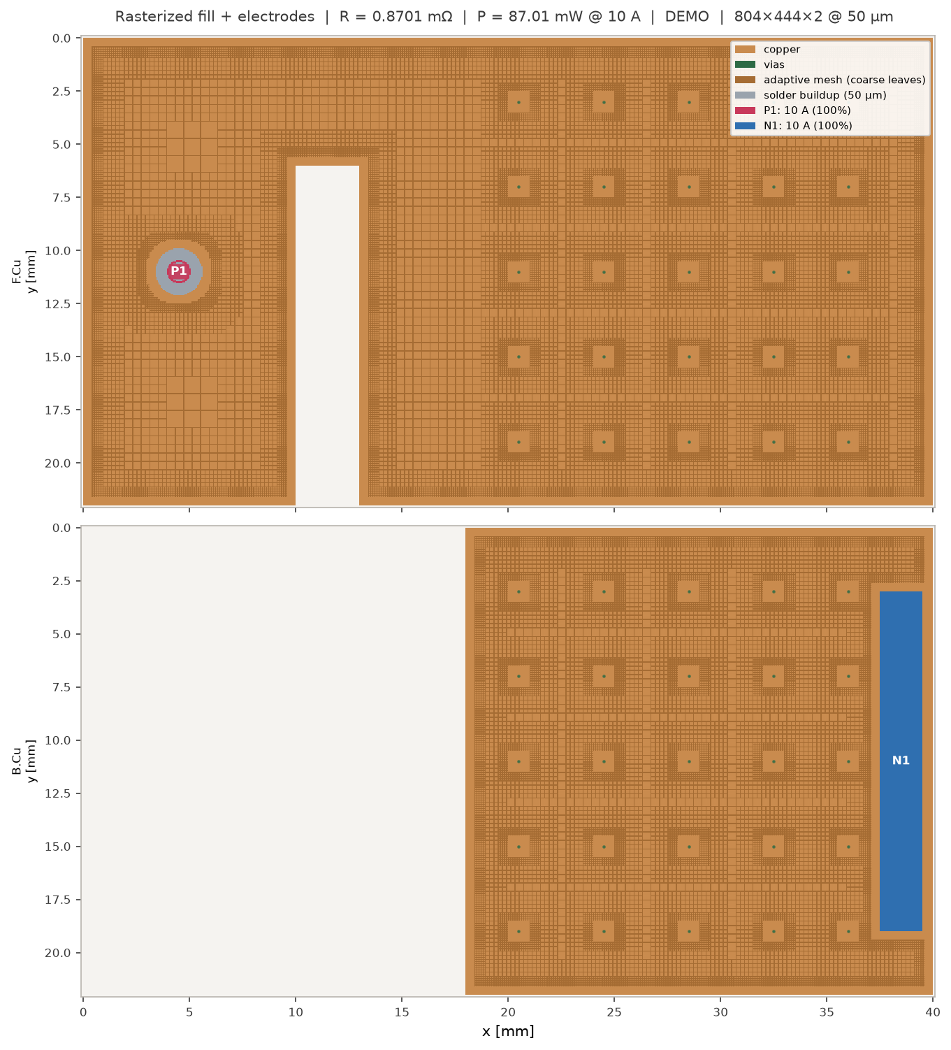 The raster map of the demo net: quadtree leaves drawn on the copper
(fine at boundaries, electrodes, via mouths and pads; coarse blocks
in plane interiors), the tin-gray solder coat of the THT-pad contact
P1, and the via field with its pad copper.
The raster map of the demo net: quadtree leaves drawn on the copper
(fine at boundaries, electrodes, via mouths and pads; coarse blocks
in plane interiors), the tin-gray solder coat of the THT-pad contact
P1, and the via field with its pad copper.


Measured vs. computed: we tested the plugin on a few real boards against a UT3513+ micro-ohm meter; the measured resistances were within ±20 % of the computed values. We attribute the deviation to imperfections of the testing setup (probe placement and probe contact resistance vs. the ideal modeled contacts) and to manufacturing inaccuracies — actual copper and plating thicknesses routinely deviate from nominal. Relative comparisons between layout variants are accordingly more trustworthy than absolute numbers.
Offline / development
Every run writes geometry_dump.json; re-solve without KiCad:
uv run python -m fill_resistance.standalone dump.json
    [--current 40] [--cell-um 50] [--layers F.Cu,In1.Cu] [--no-show]
    [--out DIR] [--force-iterative] [--config fill_res_config.json]
    [--v-nominal 3.3]
--config applies a config file's run section as defaults under the
explicit flags (CLI wins; the dump already bakes geometry and
physics). PDN dumps (schema v8) re-solve their embedded terminal set
automatically; --v-nominal overrides the default supply open-circuit
voltage there.
Dev environment, tests, headless extraction — uv
manages the venv from pyproject.toml/uv.lock (requirements.txt
stays: KiCad builds the plugin's runtime venv from it):
uv sync                                              # one-time env setup
uv run pytest -q                                     # incl. exact analytic cases
uv run python tools/api_probe.py                     # IPC API probe vs live KiCad
uv run python -m fill_resistance.board_io dump.json [NET]  # extract only
Packaging / publishing
python tools/build_package.py builds the PCM addon zip in dist/
(installable right away via Plugin and Content Manager → Install from
File) plus dist/metadata-registry.json with the SHA-256 and sizes
filled in. To publish: upload the zip to a release, set download_url
(and the homepage resource in metadata.json), then submit the
registry copy as packages/th.co.b4l.fill-resistance/metadata.json in a
merge request to https://gitlab.com/kicad/addons/metadata. Icons are
regenerated with python tools/gen_icons.py; the README figures in
docs/img/ with uv run python tools/gen_readme_figs.py
(real solver output on small synthetic boards, plus the hand-drawn
hole cross-section).
License
GPL-3.0-or-later — see LICENSE.
Troubleshooting
- No toolbar button: venv still building (wait), or build failed →
Recreate Plugin Environment (right-click the plugin's row in
Preferences → PCB Editor → Action Plugins); check the interpreter
path (setup 2); on Linux make sure
python3-venvis installed. Last resort: delete the venv directory by hand (setup 4) and restart. - "Could not connect to KiCad's IPC API": API server not enabled, or KiCad not running (no headless mode in KiCad 10).
- "KiCad is busy": a modal dialog is open in KiCad — close it, rerun.
- Windows don't appear: they may open behind KiCad (raised best-effort); PNGs are always saved regardless.
- Result seems too low/high: remember the model is fills + barrels only, with ideal contacts; measure electrode-to-electrode.
LLM disclaimer
This plugin was developed with an LLM: Anthropic's Claude (Claude
Code, model Claude Fable 5). The physics model, solver, tests, tooling
and this documentation (including the figures; all but the hand-drawn
hole cross-section are generated by the solver itself) were written by
the model, feature by feature, under human direction and review
(janik / B4L); most commits carry a Co-Authored-By: Claude trailer.
What keeps this honest: the test suite pins the numerics to exact
analytic references (strip and annulus resistances, the acosh spreading
resistance of two circular contacts, skin-effect limits, power-balance
identities) and to convergence/regression checks; run it with
uv run pytest. Real boards were measured against a UT3513+ micro-ohm
meter (see Measured vs. computed above). Nevertheless, an LLM wrote
this: read Model & limits
critically, treat surprising numbers with the usual engineering
suspicion, and cross-check against a hand estimate before trusting a
result with hardware. Bug reports are very welcome.